當(dāng)前位置:首頁 > 產(chǎn)品中心 > 二維材料 > 二維材料薄膜 > 機(jī)械剝離單層二硒化鎢薄膜


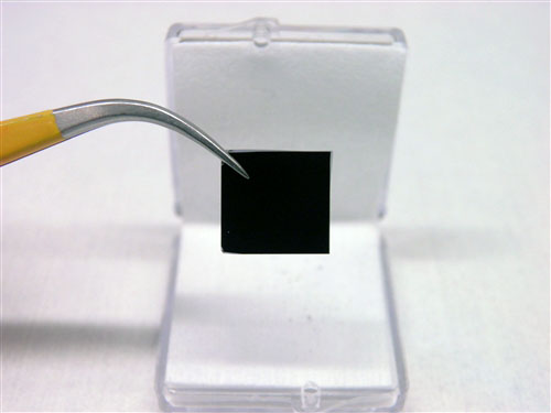
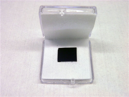
簡要描述:Monolayer tungsten diselenide (1H-WSe?) flakes have been exfoliated from bulk tungsten diselenide (2H-WSe?) onto 90nm thermal oxide and measures from 5micron up to 40micron in size.
 產(chǎn)品型號(hào):
  廠商性質(zhì):生產(chǎn)廠家
 更新時(shí)間:2024-06-03
 訪 問 量:891
相關(guān)文章
Related Articles詳細(xì)介紹
Monolayer tungsten diselenide (1H-WSe?) flakes have been exfoliated from bulk tungsten diselenide (2H-WSe?) onto 90nm thermal oxide and measures from 5micron up to 40micron in size. Each sample contains at least one single-layer WSe? and is easy to find with the given x and y coordinates. Full characterization is performed on each monolayer flake. Typically, single-layer WSe? show strong PL at 1.66eV with 0.04 to 0.08eV FWHM, and the Raman peaks are located at 139.5cm-1 (E2g in-plane mode) and 249.5 cm-1 (A1g out-of-plane mode). All the data is provided with the sample and data includes Raman, photoluminescence, 100x optical images, and x,y coordinates.
Characterization
Raman spectroscopy: Raman spectroscopy is data is taken on every single-layer flakes. Typically, flakes show two prominent Raman peaks at 139.5cm-1 (E2g- in plane-) and 249.5cm-1 (A1g out-of-plane) and the FWHM (full-width-at-half-maximum) is less than 5cm-1. Photoluminescence (PL): In the single layer form, tungsten diselenide possesses direct band-gap at 1.65eV. PL measurements show strong PL peak located at 1.66eV with 0.04-0.08 eV PL FWHM.
Optical Microscope images: Each sample is inspected under the optical microscope and x-y coordinates are recorded.
Contact us for more information
Possible applications:
Electronics
Sensors - detectors
Optics
STM - AFM applications
Molecular detection - binding
Ultra-low friction studies
Materials science and semiconductor research


產(chǎn)品咨詢
聯(lián)系我們
上海巨納科技有限公司 公司地址:上海市虹口區(qū)寶山路778號(hào)海倫國際大廈5樓 技術(shù)支持:化工儀器網(wǎng)掃一掃 更多精彩

微信二維碼

網(wǎng)站二維碼